


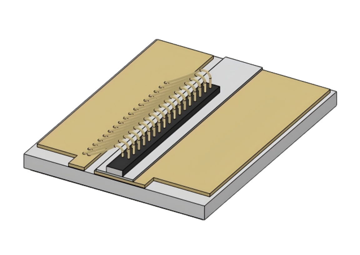
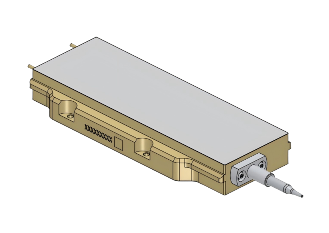
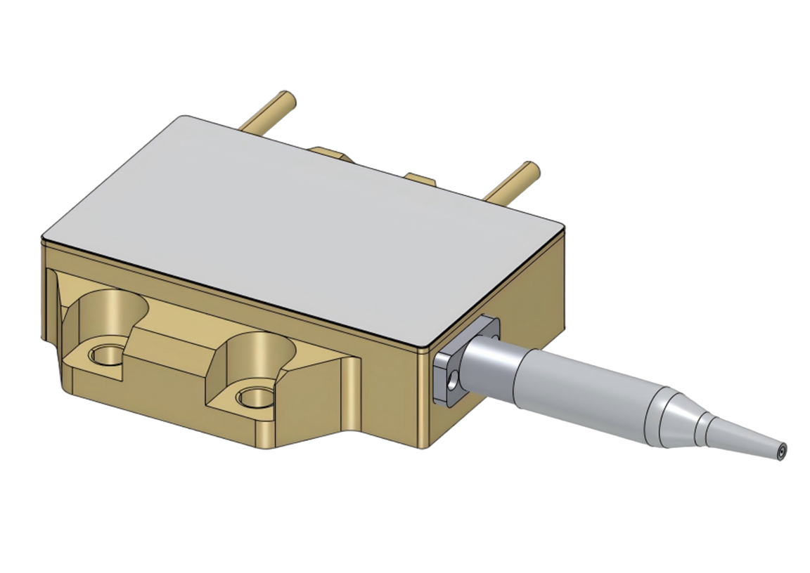
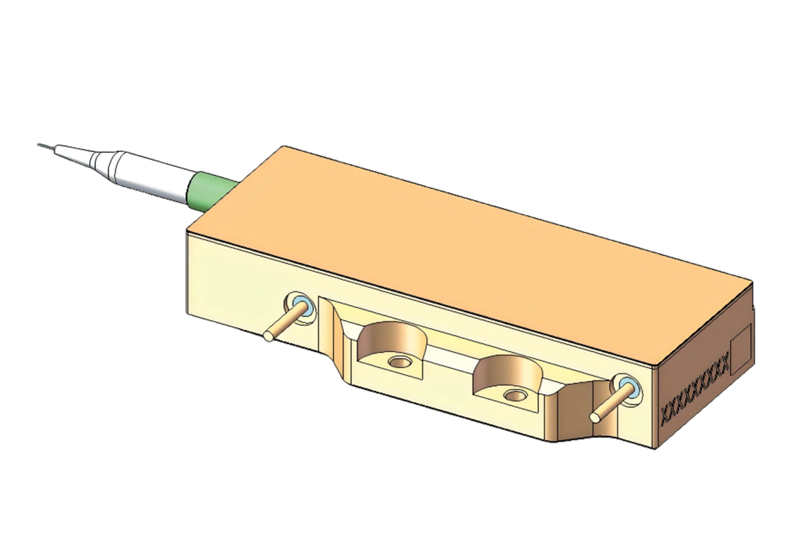
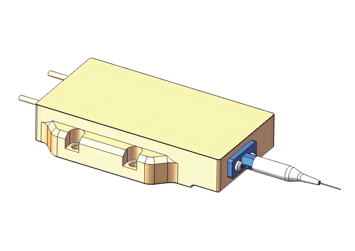
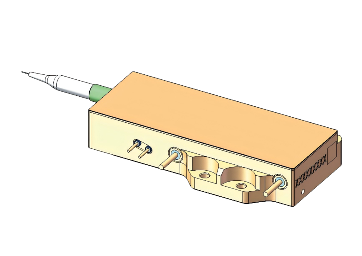
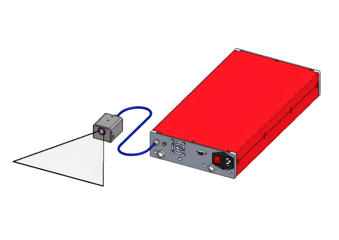
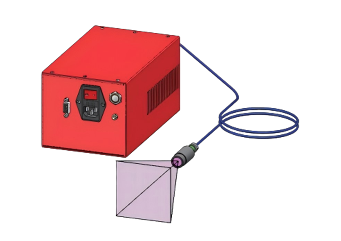
30W-200W Semiconductor Laser
30W/50W/200W PL inspection is a non-contact detection method based on optical excitation and high-sensitivity camera imaging, widely used for quality inspection of silicon wafers, solar cells, and other semiconductor materials.
-
30/50/200WOutput Power
-
808±5/915±10nmCentral Emission Wavelength
-
10nmSpectral Width

-
Product Advantages
-
Specification
-
Related Products
Product Advantages
-
Non-Contact Inspection
The PL method ensures zero physical damage or contamination to silicon wafers, preserving sample integrity during inspection.

-
High Sensitivity
Capable of detecting micron- and even nano-scale defects and impurities, with significantly higher sensitivity than conventional inspection methods.
-
High Throughput
Enables rapid processing of large sample volumes, dramatically improving production efficiency and quality control performance.
Specification
-
JPT-30W


-
JPT-50W

-
JPT-200W

-
Output Power(W)
-
Central Wavelength(nm)
-
Center Wavelength Deviation
-
Typical Working Distance(mm)
-
Detectable Wafer Size(mm)
-
Power Requirements(V)
-
IO Interface(V)
-
Average Power Consumption(W)
-
Beam Emission Control
-
Power Regulation Mode
-
Operating Temp.&Rh(℃)
-
Dimension(mm)
-
Weight(kg)
-
Applicable Technology
-
Cooling
-
JPT-30W
-
Output Power(W)30
-
Central Wavelength(nm)808
-
Center Wavelength Deviation±5
-
Typical Working Distance(mm)230~260
-
Detectable Wafer Size(mm)≤230
-
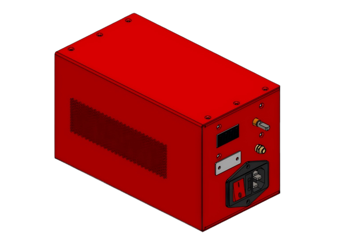
Power Requirements(V)220
-
IO Interface(V)White 0~24+/ Black 0~0.5-
-
Average Power Consumption(W)100
-
Beam Emission ControlIO Interface
-
Power Regulation ModeGUI
-
Operating Temp.&Rh(℃)20~30;<80%
-
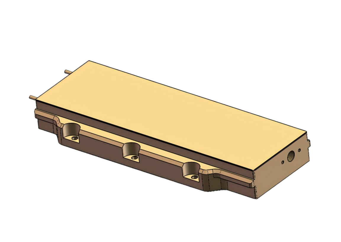
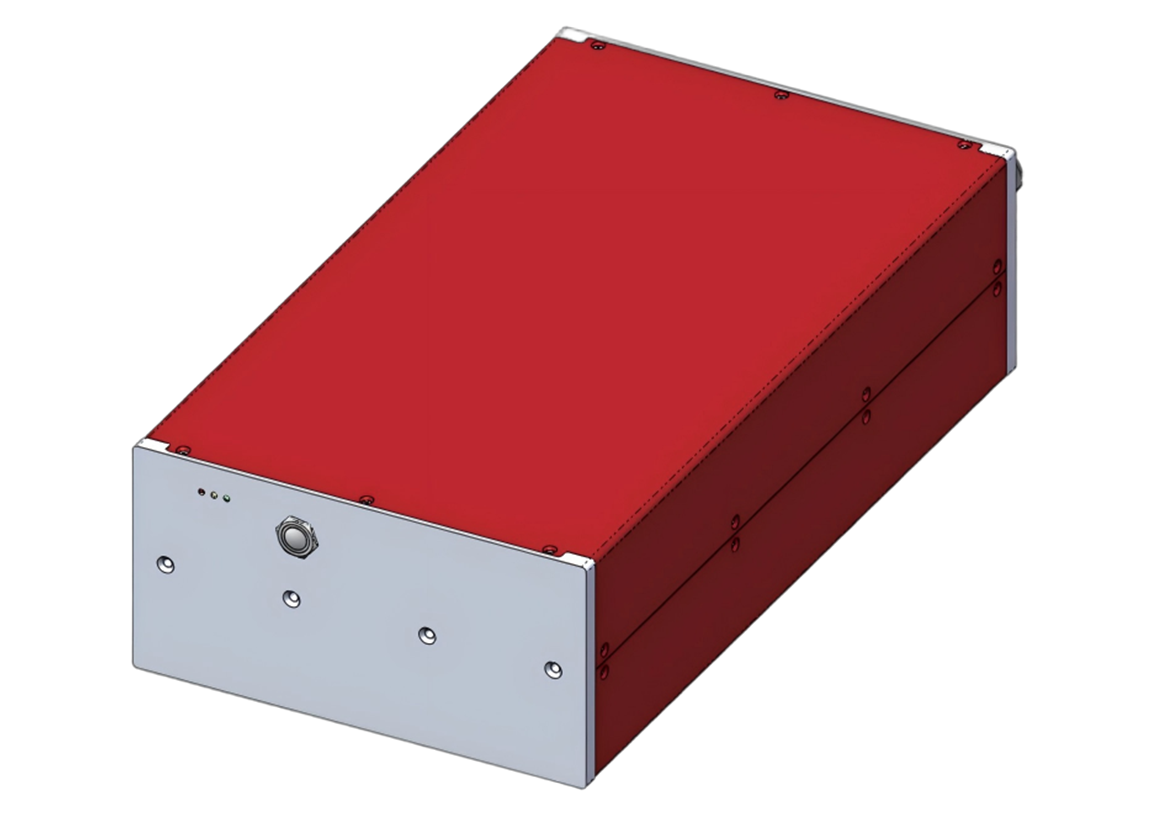
Dimension(mm)205×111×123
-
Weight(kg)≈4
-
Applicable TechnologyProcess After Silicon Wafer Coating
-
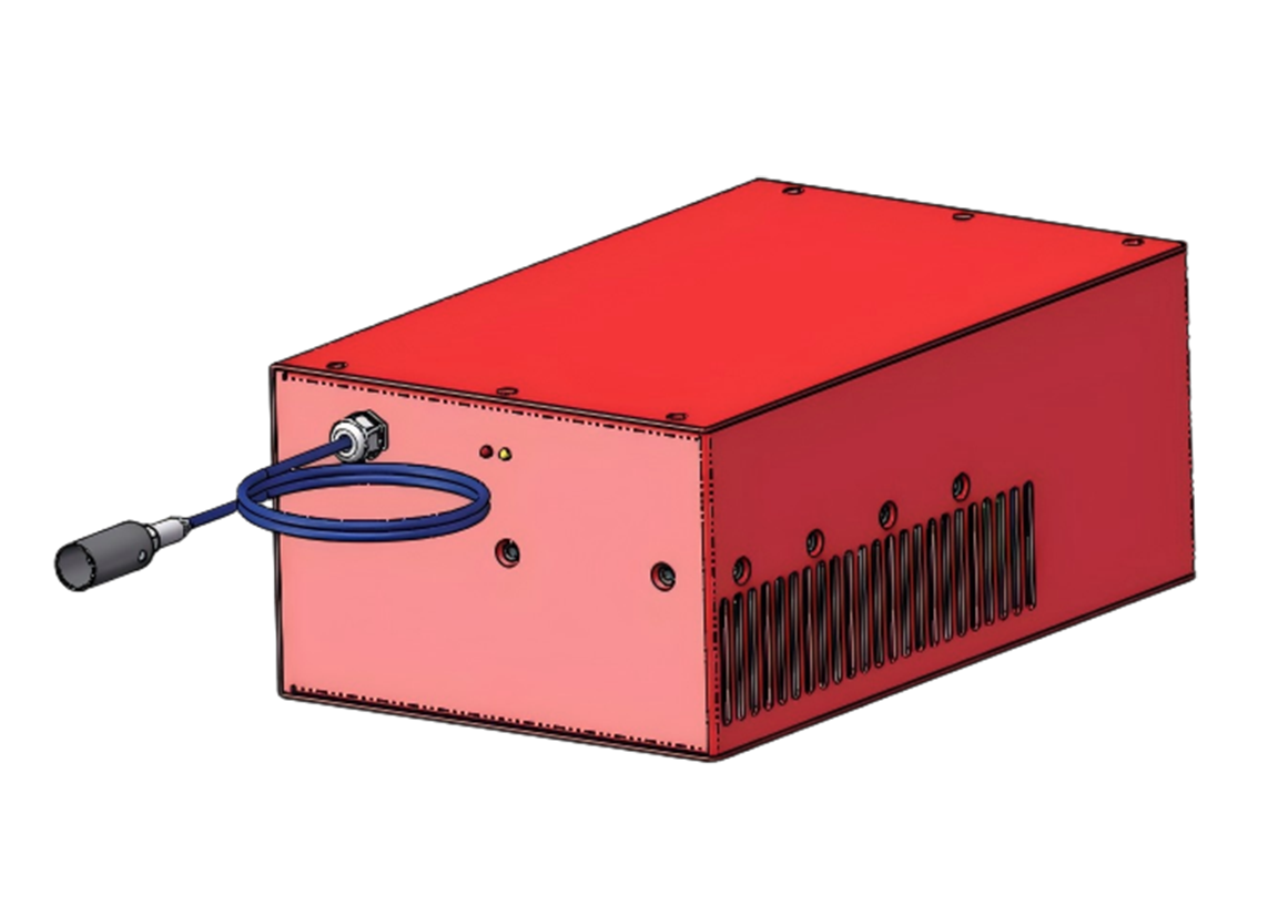
CoolingAir-Cooled
-
-
JPT-50W
-
Output Power(W)50
-
Central Wavelength(nm)808
-
Center Wavelength Deviation±5
-
Typical Working Distance(mm)230~260
-
Detectable Wafer Size(mm)≤230
-
Power Requirements(V)220
-
IO Interface(V)White 0~24+/ Black 0~0.5-
-
Average Power Consumption(W)130
-
Beam Emission ControlIO Interface
-
Power Regulation ModeGUI
-
Operating Temp.&Rh(℃)20~30;<80%
-
Dimension(mm)232×140×122
-
Weight(kg)≈5
-
Applicable TechnologyProcess After Silicon Wafer Diffusion
-
CoolingAir-Cooled
-
-
JPT-200W
-
Output Power(W)200
-
Central Wavelength(nm)915
-
Center Wavelength Deviation±10
-
Typical Working Distance(mm)230~260
-
Detectable Wafer Size(mm)≤230
-
Power Requirements(V)220
-
IO Interface(V)White 0~24+/ Black 0~0.5-
-
Average Power Consumption(W)560
-
Beam Emission ControlIO Interface
-
Power Regulation ModeGUI
-
Operating Temp.&Rh(℃)20~30;<80%
-
Dimension(mm)450×235×70
-
Weight(kg)≈10
-
Applicable TechnologySubsequent Processes of Silicon Wafers
-
CoolingWater-Cooled
-
Related Products
-

 COS Encapsulated Semiconductor Laser
COS Encapsulatedtechnology offers high efficiency, low thermal resistance, and enhanced reliability, applicable in industrial processing, medical equipment, and communications fields
-
 915nm Semiconductor Laser
Suitable for fiber laser pumping applications across industrial processing, medical, cosmetic, and scientific research sectors
-
 976nm Semiconductor Laser
Near-infrared laser equipment, used as a pump source for fiber lasers
-
 808nm Semiconductor Laser
Near-infrared lasers serving as solid-state laser pumping sources
-
 880nm Semiconductor Laser
High-efficiency laser equipment in the near-infrared band, also serving as a pump source for solid-state lasers
-
 1060nm Semiconductor Laser
Used for quality inspection of silicon wafers, solar cells, and other semiconductor materials
-
 1470nm Semiconductor Laser
High efficiency and excellent stability, 1470nm widely used in medical, cosmetic, and scientific research fields
-
 1550nm Red Light Semiconductor Laser
High-power, visible light marking, widely used in material processing, medical equipment, and scientific research experiments
-
 450nm - 100W High Power Diode Laser
Utilizing blue laser wavelengths, it features high output power, excellent stability, and high efficiency
-
 Silicon Transmission Series Detection Module
Widely used for quality inspection of silicon wafers, solar cells, and other semiconductor materials
-
 200W Red Light Series Semiconductor Laser
Widely used in material processing, medical equipment, and scientific research experiments
-
 30W Fiber Coupled High Power Laser
Utilizing blue light wavelengths, applied in material processing, display technology, laser imaging, etc.
-
 30W-200W Semiconductor Laser
Used for quality inspection of silicon wafers, solar cells
-
 50W Square Light Semiconductor Laser
Utilizes a fiber-coupled diode laser source with integrated precision control circuitry