


Pan-Semiconductor
JPT integrates core laser and automation technologies for wafer trimming, ceramic cutting, glass drilling, and marking. Our high-performance lasers and intelligent equipment enhance precision, yield, and process consistency across MLCC, LTCC, and IC substrates.


-
Wafer Resistor Trimming
-
Ceramic Substrate Cutting
-
Wafer Laser Processing
-
Module Testing Applications
-
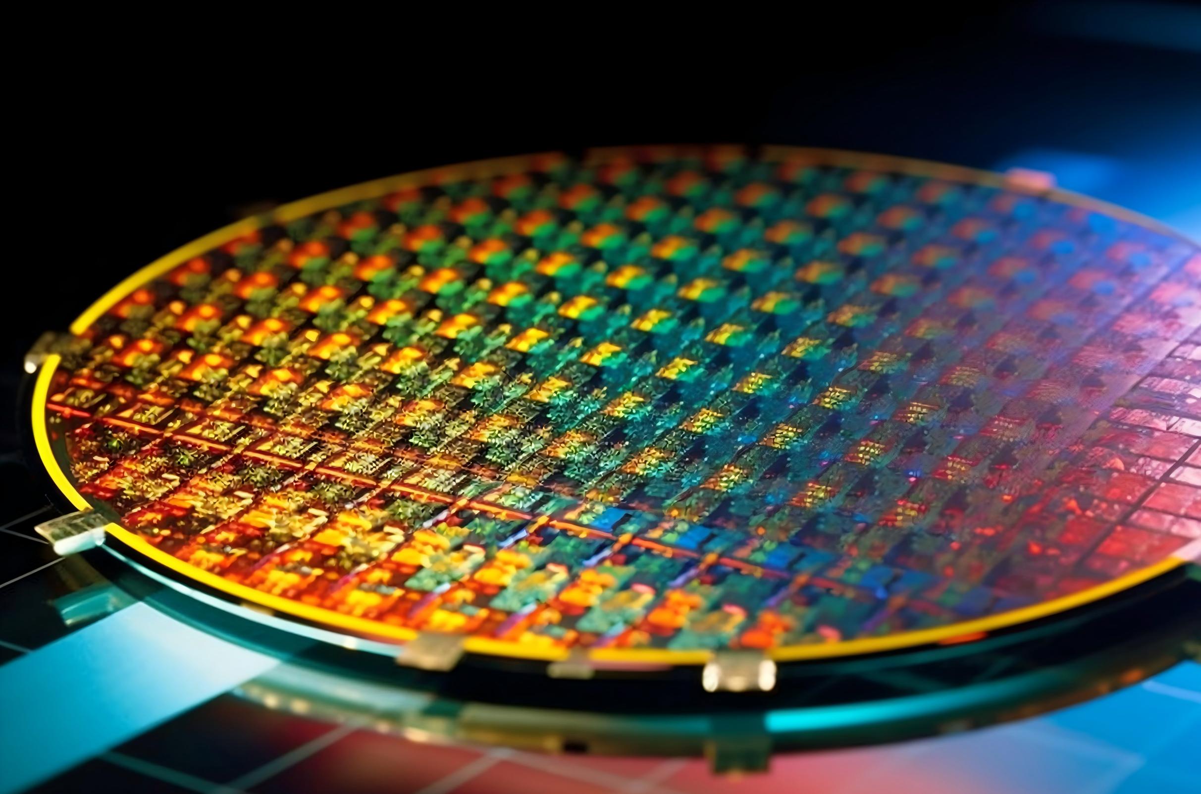 Wafer Resistor Trimming
In semiconductor wafer testing and passive component tuning, precision resistor trimming is vital to product consistency and yield. JPT’s proprietary wafer trimming systems integrate high-precision UV lasers, motion platforms, and measurement systems, supporting a broad resistance range (100 mΩ to 1 GΩ) with ±0.01% trimming accuracy. Featuring automatic wafer recognition, probe positioning, and pattern detection, these systems support multiple blade path types and wafer sizes (4" to 8"), ideal for ADC chips, power management ICs, RF chips, and resistor networks.
-
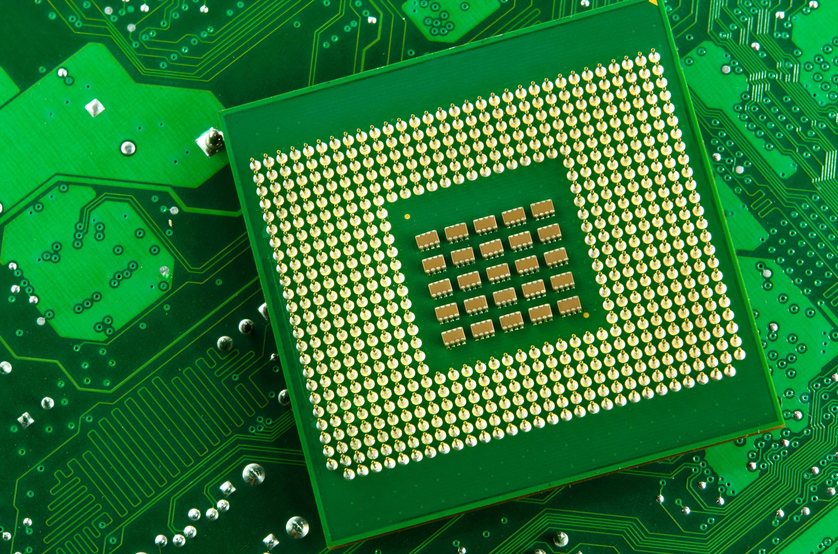 Ceramic Substrate Cutting
For MLCC, LTCC, and other passive components, efficient and damage-free ceramic cutting is key to product performance and yield. JPT offers precision green- and UV-laser cutting solutions with minimal heat-affected zones and smooth, crack-free edges—ideal for high-frequency, high-speed circuit boards and 5G ceramic filters. Fully automated loading/unloading and vision positioning modules enable high-volume, high-yield, cost-effective production.
-
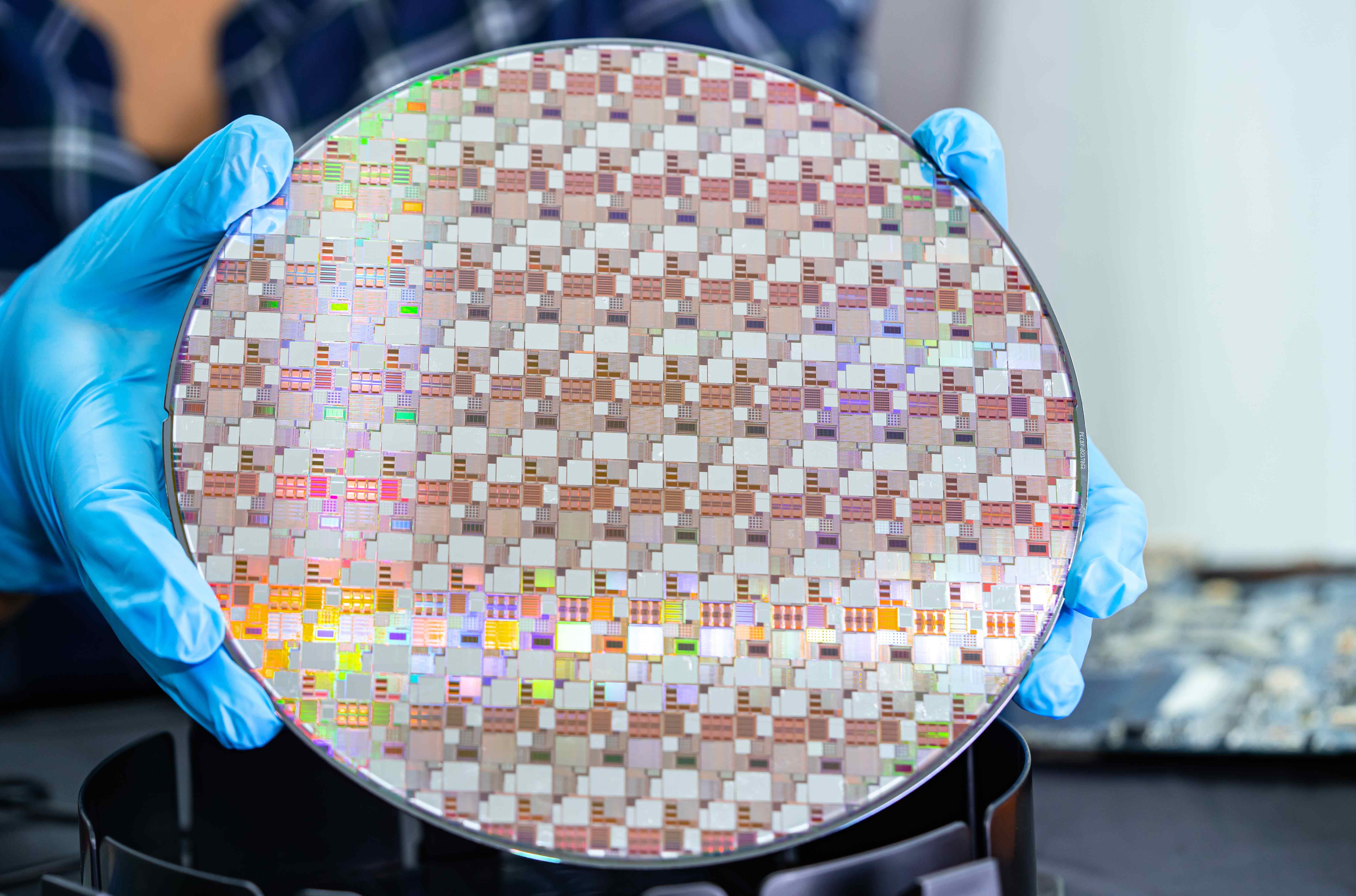 Wafer Laser Processing
JPT's wafer processing systems integrate self-developed lasers, galvanometers, and optical focusing units, with flexible automation options to handle various incoming material formats and product sizes. High-precision vision positioning and multi-surface processing capabilities ensure optimal quality and consistency. Automated sorting and NG product recovery further improve production efficiency, making laser processing an essential step in modern wafer manufacturing.
-
 Module Testing Applications
Our advanced module testing solutions cover silicon photonics, VCSEL inspection, and LED/PD performance screening. Capable of high-throughput wafer-level scanning, these systems enable simultaneous optical and electrical testing for silicon photonics chips and LiDAR modules. LED/PD platforms support Mini/Micro LED uniformity checks and receiver linearity/SNR tests, while VCSEL testers focus on optical parameters, thermal stability, and 3D sensing calibration—serving consumer electronics, automotive LiDAR, and industrial VCSEL applications.