Table of Contents
Marking in packages is not new. These marks may be some text, codes, logo or product related images. At present, Laser based marking dominates over any other conventional marking method due to its some special characteristics such as it is straightforward to use, repeatability, non-contact, fast and precise processing etc. It also offers great flexibility as it can be modified according to one’s need.
Challenges for laser marking in packaging industry
Laser based marking is superior and still evolving. It faces many challenges in diverse packaging field. The condition of poor markability may arise due to difficulty in marking precisely or marks are not long lived. There may be various reasons for these failures. Some issues are illustrated here with:
Marking pattern may not be clear due to following reasons
- mold base is non-uniform
- mold pressure is not proper
- laser induced temperature rise may not be enough
So, materials characteristics and laser parameters should be adjusted before actual marking could take place.
Contrast issue in paper and cardboard marking
Laser marking paper and cardboard is done through the vaporization of thin layer of same material. This kind of mark does not change the color but same color gives lighter appearance. The contrast of this kind of marks is not very good. The contrast of such marks can be improved by absorbing surface coating of contrasting colors. These coatings can be selectively removed exposing the color of paper or cardboard creating the good contrasting marks.
Metal additives in Plastic Marking
Plastic marking with IR laser has been very popular especially in 1.06 um wavelength range. But to achieve enough absorption in this wavelength, metal additives are mixed with plastics. These metal additives are very harmful for plastic products used in food packaging. One good option to avoid these metals additives can be to use UV laser in place of IR lasers. UV lasers can be directly used to mark on plastic with no need to use any metal additives.
Shallow marking for semiconducting devices
The enclosures in Integrated Circuit Packaging is thick enough to allow deep marking. However, in some semiconducting devices, deep marking is not possible due small thickness of enclosure material. Enclosure of epoxy material are highly absorbing at green wavelength and therefore Green laser can be used for shallow marking in semiconducting device marking.
Marking in defocused target
It is very important that material surface is at laser focus to get efficient mark. But there are situations when materials surface goes out of focus again and again. For example, in step marking, marking in inclined surface, marking in conic or cylindrical shape. In these situation, real time automatic focusing is very important and displacement sensor should be the integral of laser marking system.
Benefits of laser marking in packaging
Creating marks in packaging is not new and various marking methods were prevalent in past. But laser based marking gave that desperately required speed to this fast paced industry which was never possible before. Laser offers a great versatility and therefore, it doesn’t matter which material to be marked, a typical laser system is always available.
It offers smart and covert coding to protect from copy. Also these marks will not be wiped out so coding is permanent. Eye catching labels are very popular in beverage production. Laser induced marks offers a great flexibility to experiment with designs and these marks are also most reliable for mass production. Laser marking setup is one time investment but then the whole process is straightforward, easy to maintain and very comfortable.
Choosing the right laser for microelectronic packaging task
On the one hand lasers offer a great variability and flexibility of laser parameters so that one can tune laser system precisely according to their needs. In fact, laser technology is becoming more and more relevant as the microelectronic device size is continuously shrinking.
But the good availability of different laser system has made the selection of right one more challenging. It is very important to make wise selection of laser technology for getting optimized production output. In microelectronic packaging industry, lasers can play different role, for example, microdrilling, soldering, annealing, bonding, die separation from wafer, singulation and die sawing etc.
Accordingly, different laser systems are used such as CO2 laser, CO laser, DPSS laser, Ultrafast Laser, Excimer laser etc. Here with the following examples we can understand how different laser can be applicable for different task in microelectronic packaging.
Microvia drilling in PCB:
Short pulsed laser with peak power are the right choice to create fine few micrometer microvia hole. JPT’s DPSS lasers are more suited to metals due to good absorption at shorter wavelength. CO2 laser has been popular due to good compromise between cost and power generation.
There longer wavelength limits its use for comparatively larger diameter hole. Excimer lasers are good choice in UV range as they offer better power with good pulse repetition frequency. Ultrashort laser with short wavelengths are better choice to control heat affected zone (HAZ) with negligible effect in surrounding of the hole.
Laser Marking:
Microelectronic packaging requires marking and epoxy based molding are used. These materials show good absorption to DPSS and Fibre laser wavelengths. In case of shallow marking, Green laser are employed.
Lasers for food packaging:
Modified Atmospheric Packaging (MAP) has been used for a long time for the preservation of food. Laser perforation is comparatively newer technique that allows gas permeability to maintain freshness of the food for extended time. Traditionally polymeric films based gas permeability was not so efficient. JPT’s CO2 laser can be very efficient for laser perforation.
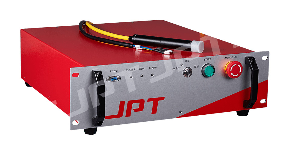
JPT offers a good selection of lasers sources that are capable of doing all kind of packaging related tasks and covers a variety of common packaging material in the market. Short pulse width with high peak power, frequency of upto 4000 khz, good power range are some attractive features of JPT laser which are known for the ease with which they can be integrated into existing production line.
Recommend Reading
Color Laser Marking Guide
Table of Contents What Exactly is Color Laser Marking? Color laser marking is the process of creating color marking on objects using laser machines. Marking
Laser Marking: Everything You Need to Know
Used exclusively by industrial manufacturers before, laser marking technology is today used by small business enterprises, makers, hobbyists, and product designers in many different ways.
