
 M7 20W-100W
 M7 200W-300W
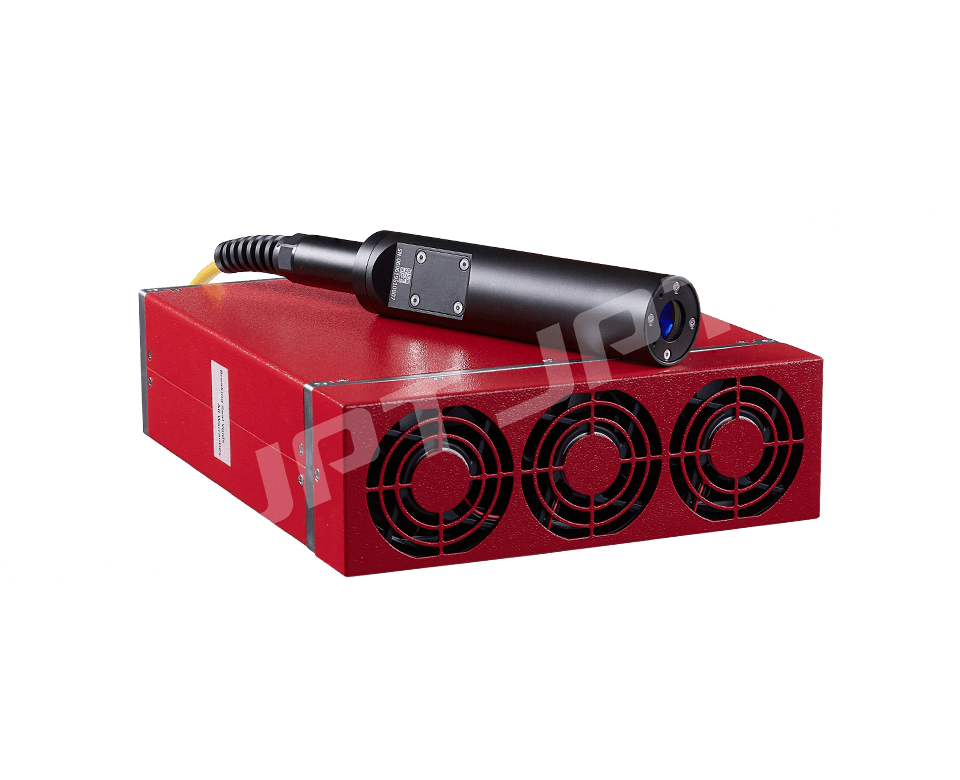
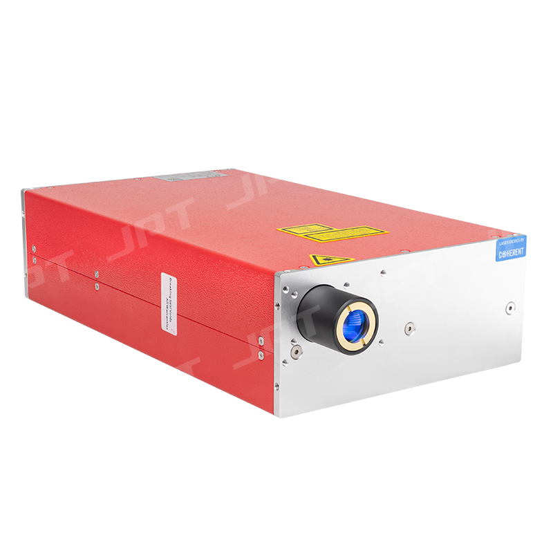
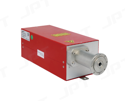
 M7 500 - 1000W
 M8 20 - 50W
 M8 120 - 300W
 CL2 200W-300W
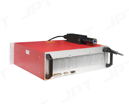
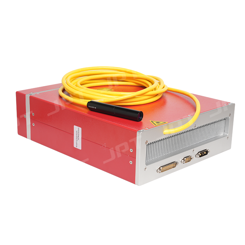
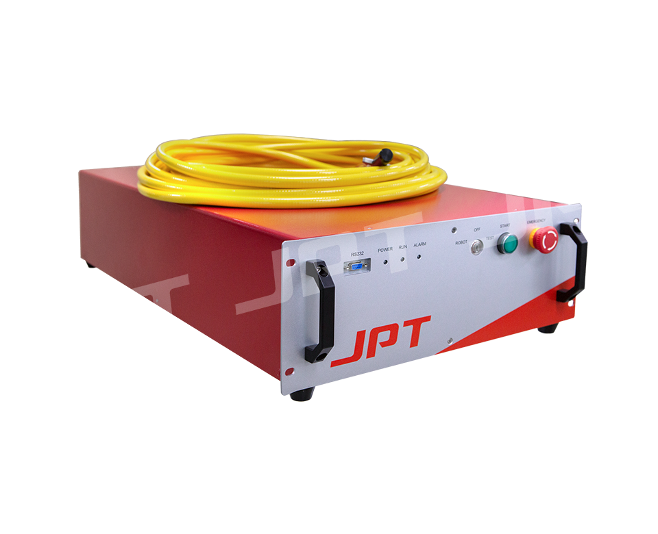
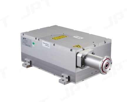
 CL 500W~1000W
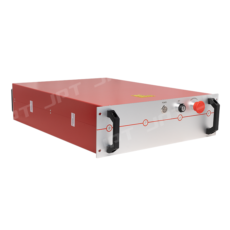
 CL 2000W
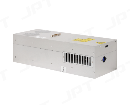
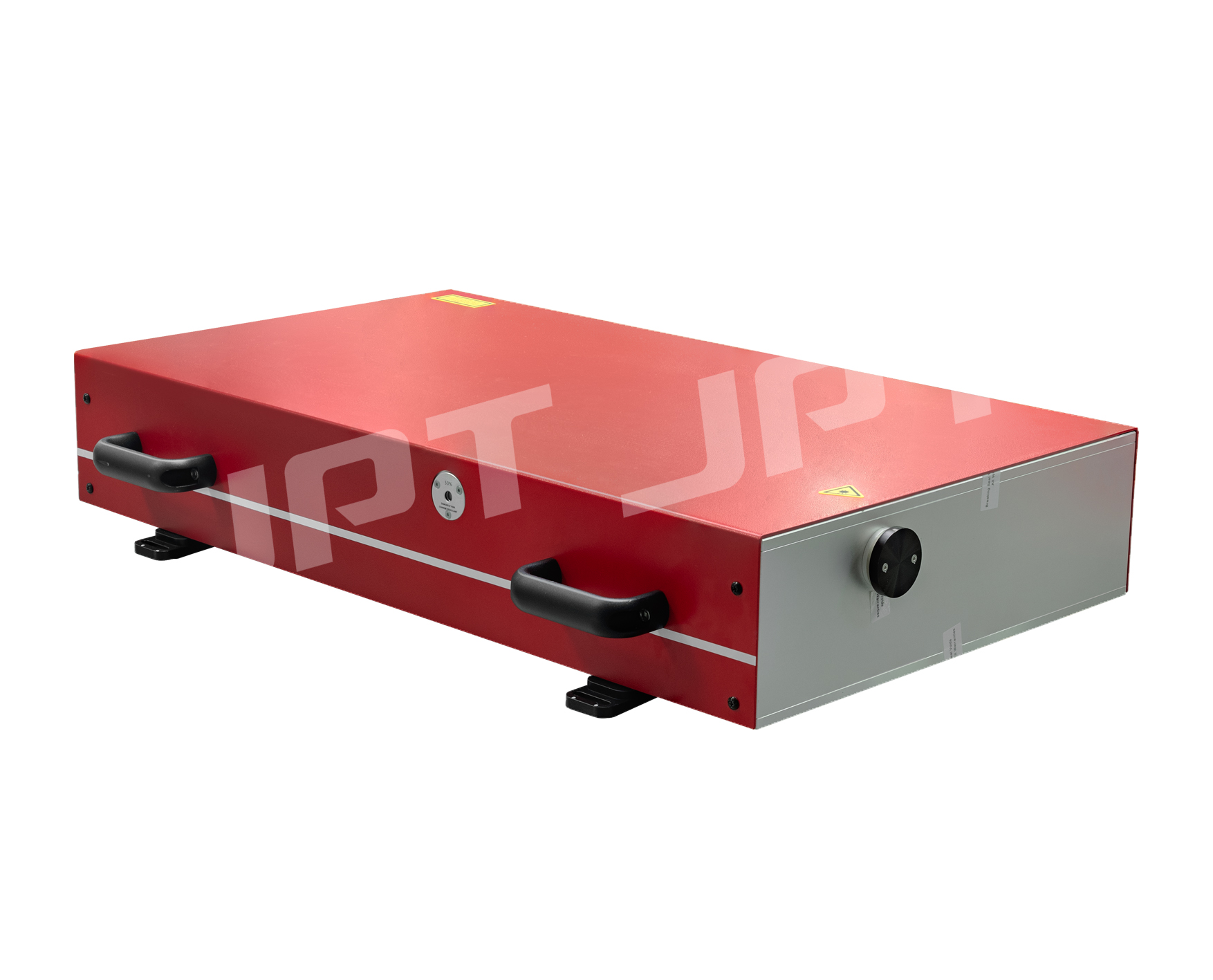
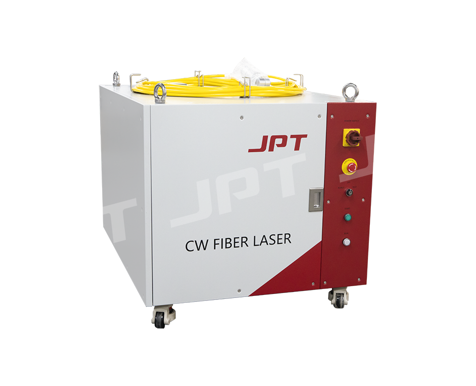 Multi-Module CW 6000W
 QCW 150W/1500W
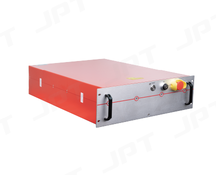
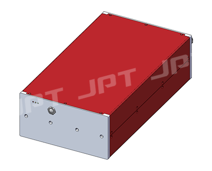
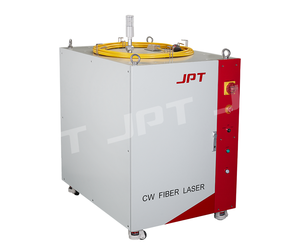 Multi-Module CW 12000W
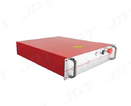
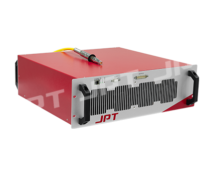
 Single-Module CW 1500W-3000W
 SEAL 355-3/5
 SEAL 532
 LARK 355-3/5
 PS IR/GR/UV Picosecond Laser
 SEAL 355-10/15/20/30
 Semiconductor Laser with Red Light Series 200W
 450nm—100W High Power Diode Laser
 10W-1064-01 Silicon Transmission Series Detection Moduler
 1060nm Series
 880nm Series
 808nm Series
 976nm Series
 915nm Series
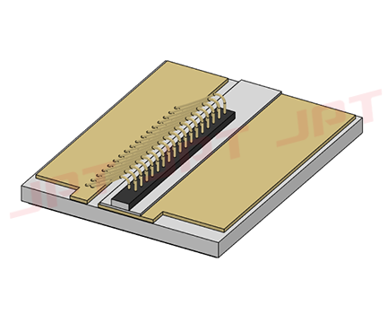 COS Encapsulated Semiconductor Laser
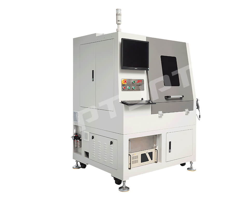
 Laser Scriber
 High Voltage Resistor Tester
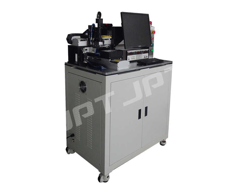 Single Chip Resistor Tester
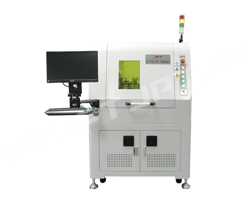 Laser Trimmer
 Hybrid Trimmer
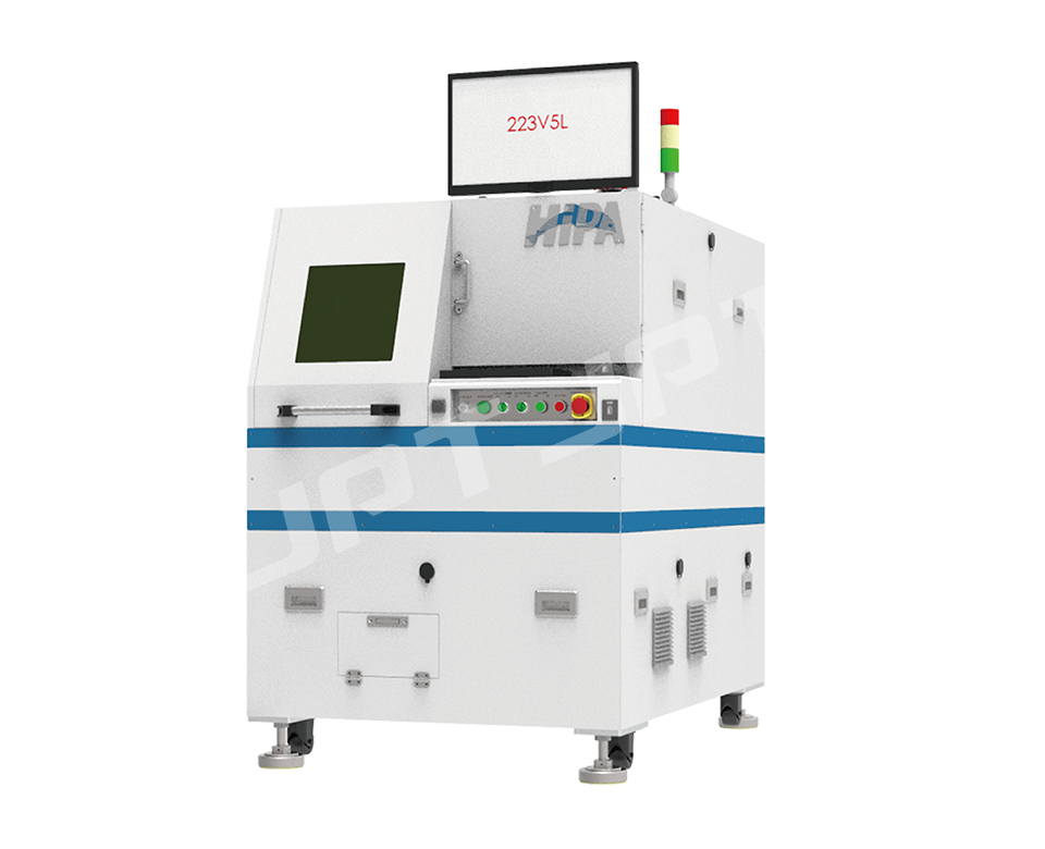
 HiPA-TT Light Transmittance Tester
 PCB Laser Marking System
 Ghost Writer & Reader - Subsurface 2D Barcode Marking & Reading System
 High Precision 2DBC Laser-marking
 Comprehensive VCSEL Module tester
 Comprehensive LED-PD Integrated Module Testing
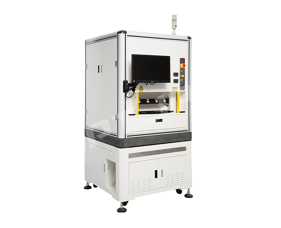
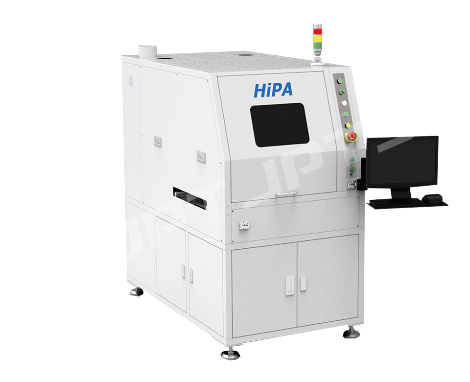
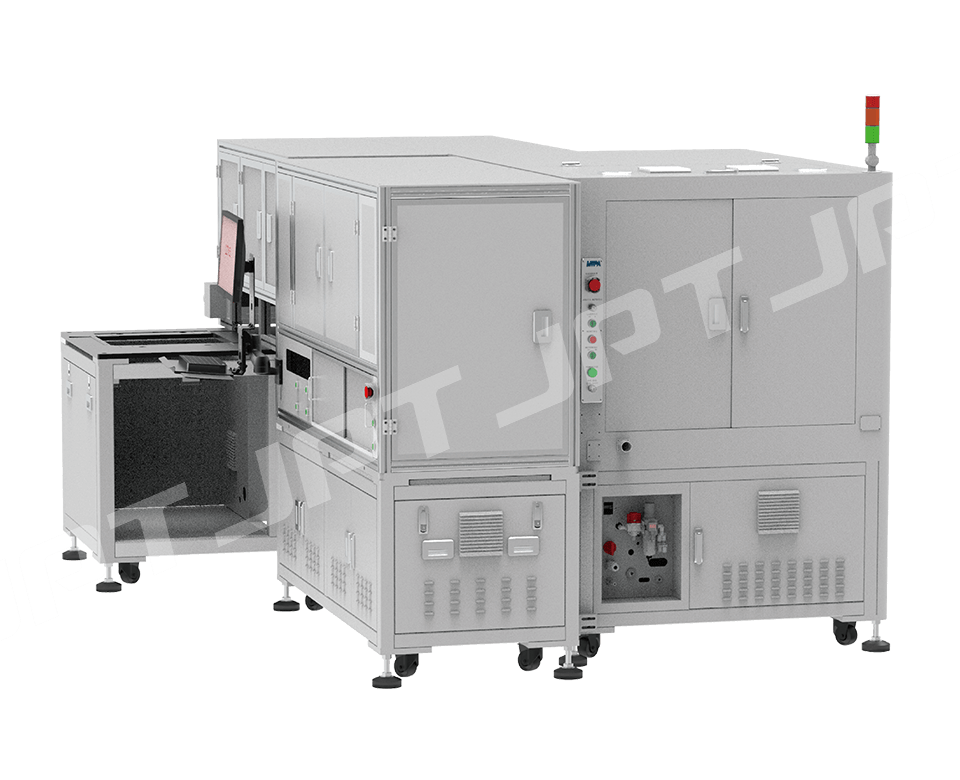
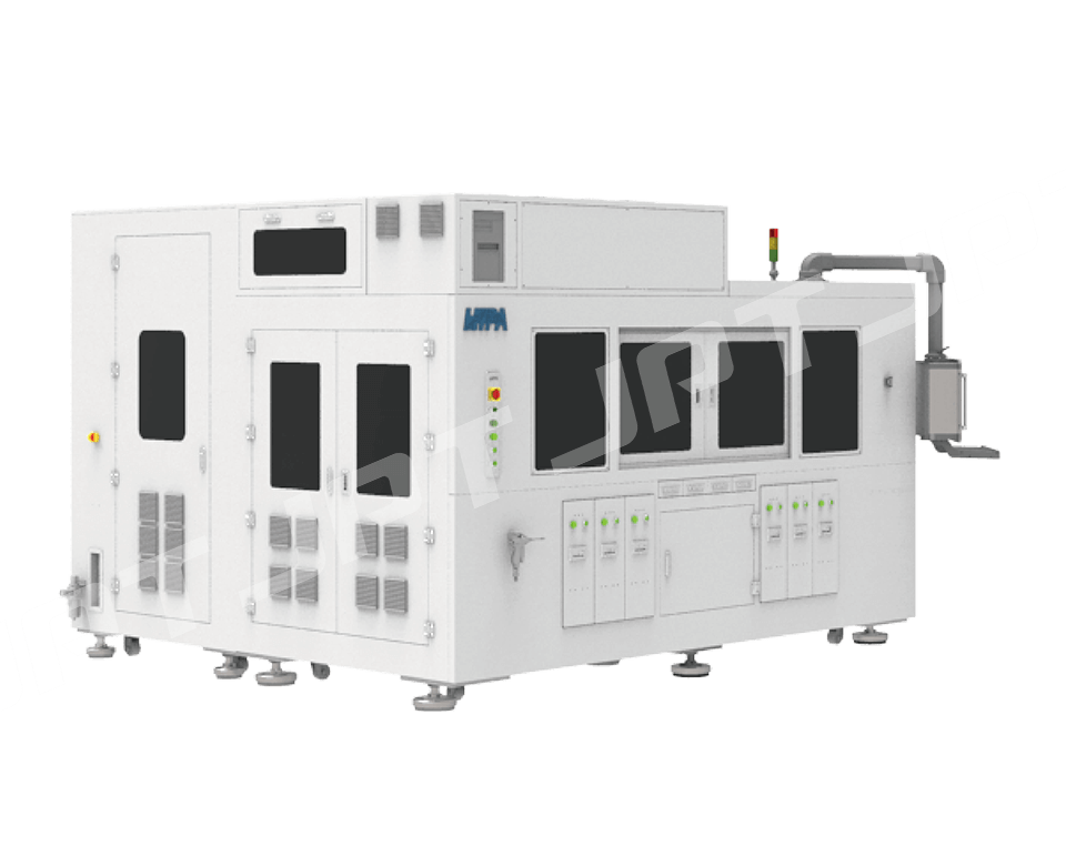
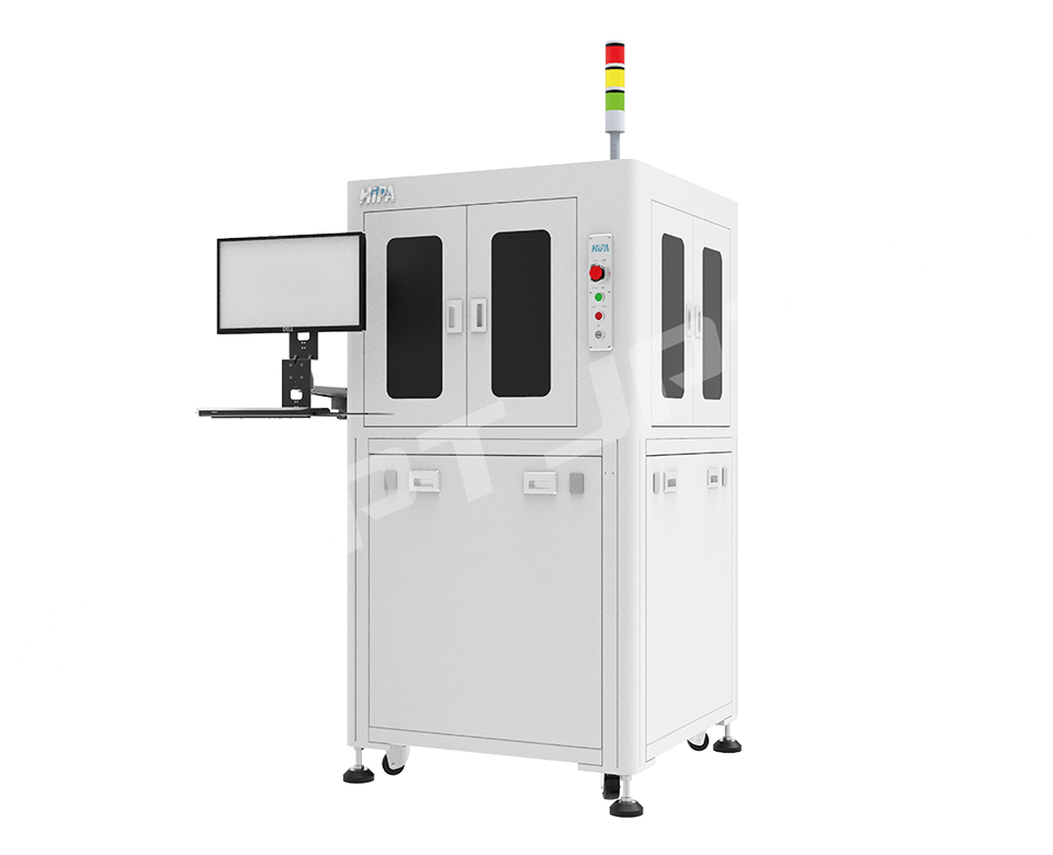 Six-sided Inspection Machine
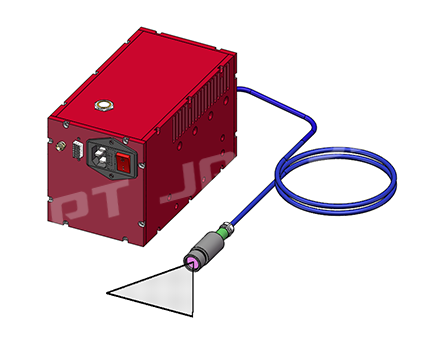
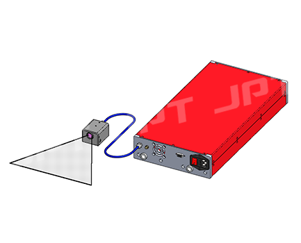
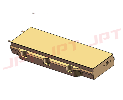
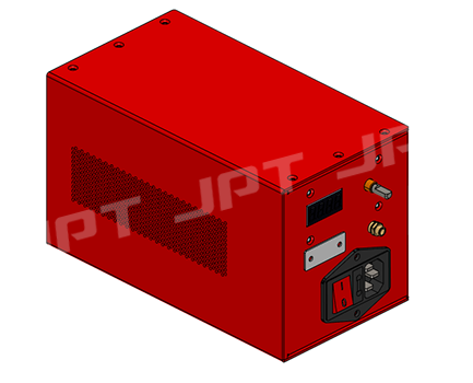
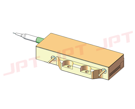
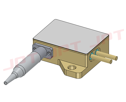
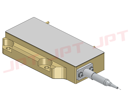
Semiconductor Laser 30/50/200W
Application Advantags
Different power output products can be customized according to customer needs
The spot uniformity is high, which is conducive to the camera's catch ffuorescence imaging
Different laser lenses can be conffgured according to different working distances
Software control out of the light easy to expand the application
JPT has different kinds of semiconductor laser components and high-power laser modules. Semiconductor laser can be widely used in pump source, industrial processing, mechanical vision, medical and many other fields. Based on the mature coupling technology solution, thermal control and packaging process, the product has the advantages of high power, high beam quality, high stability, etc., and the product wavelength covers 400nm~1000nm, which meets the special requirements of power, brightness, wavelength control, spot uniformity and so on.


JPT-30W/50W Camera capture diagram & JPT-200W Camera capture diagram
Parameter Unit | Parameter | ||
Product Model | JPT-30W | JPT-50W | JPT-200W |
Output Power | 30W | 50W | 200W |
Central Emission Wavelength | 808nm | 915nm | |
| Center Wavelength Deviation | ±5 | ±10 | |
| Typical Working Distance | 230mm~260mm | ||
The Size of the Silicon Wafer Can Be Checked | ≤230mm | ||
| Distribution Demand | 220V | ||
IO Interrace | White 0~24V+/ Black 0~0.5V | ||
Average Power Consumption | 100W | 130W | 560W |
Outgoing Light Control Mode | IO Interrace | ||
Power Regulation Mode | GUI | ||
| Operating Temp.&Rh | 20℃~30℃;<80% | ||
3D Dimensions (L×W×H) | 205×111×123mm | 232×140×122mm | 450×235×70mm |
Weight | ≈4kg | ≈5kg | ≈10kg |
Applicable Technology | Process After Silicon Wafer Coating | Process After Silicon Wafer Diffusion | Subsequent Processes of Silicon Wafers |
Cooling Method | Air-Cooled | Water-Cooled | |