Laser Application
How to Avoid Common Mistakes in Laser Engraving
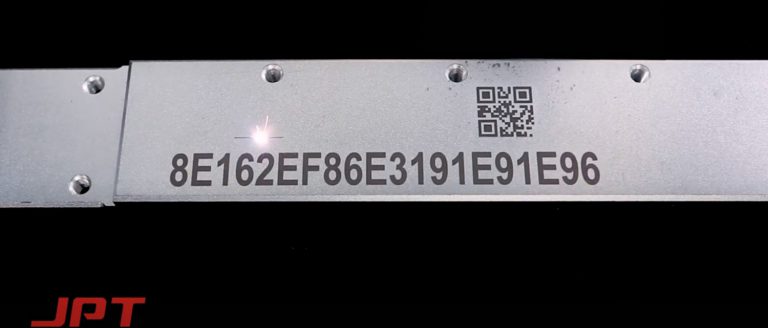
Table of Contents What is Laser Engraving? ‘Engraving’ is the process of marking by cutting the flat or curved surface generally for designing purpose. It
Laser
Laser Marking: Everything You Need to Know
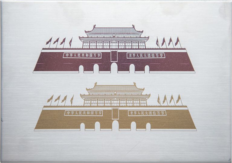
Used exclusively by industrial manufacturers before, laser marking technology is today used by small business enterprises, makers, hobbyists, and product designers in many different ways.

Latest posts by Nadir Ali (see all)